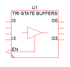
Tri-State Buffers
The tri-state buffers in the libraries are organized in banks. A single bank can be made up of one to 32 tri-state buffers. Each tri-state buffer has one input signal pin and one output signal pin. The entire bank of tri-state buffers is controlled by one enable (EN) input pin. The active logic level of the enable input pin can be configured with the Enable Level parameter.
In this topic:
| Model Name: | Tri-State Buffer | |||
| Simulator: | This device is compatible with the SIMPLIS simulator. | |||
| Parts Selector Menu Location: | ||||
| Symbol Library: | None - the symbol is automatically generated when placed or edited. | |||
| Model Library: | None - the model is automatically generated when the simulation is run. | |||
| Subcircuit Names: |
|
|||
| Symbol: |
|
|||
| Multiple Selections: | Only one device at a time can be edited. | |||
Editing the Tri-State Buffer
To configure the Tri-State Buffer, follow these steps:
- Double click the symbol on the schematic to open the editing dialog to the Parameters tab.
- Make the appropriate changes to the fields described in the table below the image.
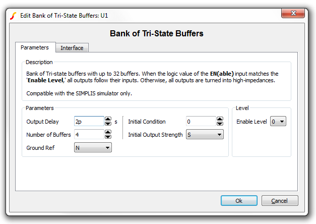
| Label | Parameter Description |
| Output Delay | Delay from when any input pin changes state until the outputs change state |
| Ground Ref | Determines whether or not a device has a ground reference pin. Any digital component that has an input or output pin connected to an analog circuit node must have its Ground Ref pin connected to an analog node. This is usually the ground on the schematic. |
| Number of Buffers | Number of tri-state buffers grouped together |
| Initial Condition | Initial condition of the entire bank of tri-state buffers at time=0. Binary value of the initial logic level of all output pins combined and then converted to the decimal equivalent. |
| Initial Output Strength | The initial output strength of all output pins. 'S' for strong and 'Z' for high-impedance. |
| Enable Level | The logic level of the enable (EN) pin at which the tri-state buffers are enabled.
|
To define the parameters for the interface between this digital component and each analog component connected directly to an input or output pin, follow these steps:
- From the Edit Tri-State Buffer dialog box, click on the Interface tab.
- Make the appropriate changes to the fields described in the table below the image.
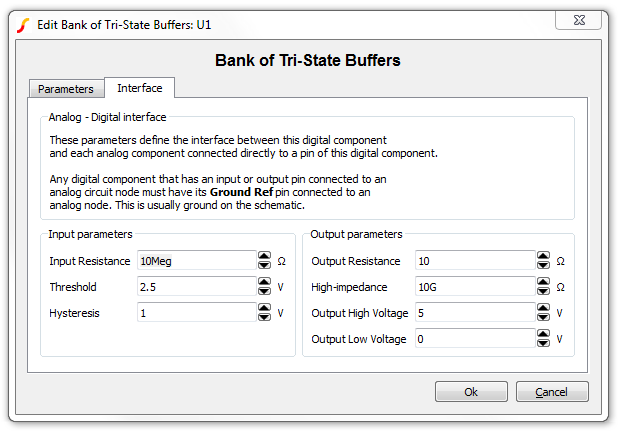
| Label | Parameter Description | |||||||
| Input Resistance | Input resistance of each Buffer input pin | |||||||
| Hysteresis, Threshold | 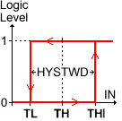 |
Hysteresis and
Threshold of the inputs. The hysteretic-window width, HYSTWD
is centered around Threshold (TH) voltage. To
determine the actual threshold ( TL , THI ),
substitute Threshold (TH) and Hysteresis
(HYSTWD) in each of the following formulas:
|
||||||
| Output Resistance | Output resistance of each Buffer output pin | |||||||
| High-Impedance | High-impedance of output resistance of each output pin. | |||||||
| Output High Voltage | Output high voltage for each Buffer output pin | |||||||
| Output Low Voltage | Output low voltage for each Buffer output pin | |||||||
Truth Table
| Inputs | Output State | |
| Signal | Enable | |
| 0 | 0 | XZ (Unknown logic level, high-impedance output strength) |
| 0 | 1 | 0S (Low logic level, strong output strength) |
| 1 | 0 | XZ (Unknown logic level, high-impedance output strength) |
| 1 | 1 | 1S (High logic level, strong output strength) |
Examples
The test circuit used to generate the waveform examples in the next section can be downloaded here: simplis_tri_state_buffer_example.sxsch.
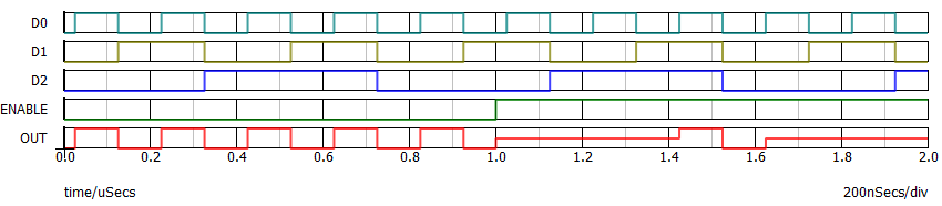
Waveforms
The waveforms below were taken from the simplis_tri_state_buffer_example.sxsch schematic, which involves a single bank of two tri-state buffers. Due to the way this test circuit is set up, the logic level of the OUT node will follow the logic level of the non-inverted output pin of U4 whenever the bank of tri-state buffers is disabled. When the bank of tri-state buffers is enabled, the logic level of the OUT node is equal to the logic level of D0 if the logic levels of D0, D1, and D2 are identical and it is equal to UNKNOWN (X) logic level otherwise.
Subcircuit Parameters
Because the model for the tri-state buffers is generated by a template script when the simulation is executed, a hand-coded model cannot be inserted into a netlist. The template script for this device is simplis_make_tri_state_buffer_model.sxscr. The following parameter table defines the parameters used in this model.
| Parameter Name | Label | Data Type | Range | Units | Parameter Description | |||||||
| ENABLE_LEVEL | Enabling Level | Number |
|
none | The logic level of the enable (EN) pin at which the tri-state buffers are enabled. 1 means enabled on logic high. 0 means enabled on logic low. | |||||||
| GNDREF | Ground Ref | String |
|
none | Determines whether or not a device has a ground reference pin. Any digital component that has an input or output pin connected to an analog circuit node must have its Ground Ref pin connected to an analog node. This is usually the ground on the schematic. | |||||||
| HYSTWD, TH |
Hysteresis, Threshold |
Number | min: 1f | V | |
Hysteresis and Threshold of
the inputs. The hysteretic-window width, HYSTWD is centered
around Threshold (TH) voltage. To determine the actual
threshold ( TL , THI ), substitute Threshold
(TH) and Hysteresis (HYSTWD) in each of the
following formulas:
|
||||||
| IC | Initial Condition | Number | none | Initial condition of the tri-state buffer output at time=0. The logic level of each output pin can be 0 or 1, depending on whether the logic level is LOW or HIGH, respectively, at t=0. To arrive at the initial condition, a binary word is constructed from the initial logic levels of all output pins, with pin O0 being the least significant bit. The decimal equivalent of this binary word should then be entered as the IC parameter. If the "initial output strength" of the tri-state buffer is set to Z (high-impedance), then the IC parameter will be ignored by SIMPLIS and the logic level of all output pins are set to X (UNKNOWN) at t=0 by the simulator. | ||||||||
| IC_OUT_STRENGTH | Initial Output Strength | String |
|
none | The initial output strength of all output pins. Set to 'S' for strong and 'Z' for high-impedance. | |||||||
| NUM_BUFFERS | Number of tri-state buffers | Integer | 1 to 32 | none | Number of tri-state buffers grouped together | |||||||
| OUT_DELAY | Output Delay | Number | 1f to 1024 | s | Delay from when any input pin changes state until the outputs change state | |||||||
| RIN | Input Resistance | Number | min: 100 | Ω | Input resistance of each tri-state buffer input pin | |||||||
| ROUT | Output Resistance | Number | min: 1m | Ω | Output resistance of each tri-state buffer output pin when the tri-state buffers are enabled. | |||||||
| ROUT_HIGH_Z | Output High Impedance | Positive Number | min: At least 10 times larger than ROUT | Ω | The output resistance of each output pin when the tri-state buffers are disabled. | |||||||
| VOH | Output High Voltage | Number | any | V | Output high voltage for each tri-state buffer output pin | |||||||
| VOL | Output Low Voltage | Number | any | V | Output low voltage for each tri-state buffer output pin | |||||||