Application B - Modeling and Measuring Power Stage Efficiency
This application topic addresses the fundamentals and best practices of Piecewise Linear modeling and loss measurement of key power-stage components in switching power supplies.
Beginning with switch stresses and losses, we examine the critical elements of MOSFET models and MOSFET driver models. We explain why these two devices need to be addressed simultaneously in order to achieve accurate simulation results. We illustrate methods for measuring total power switch losses as well as a straightforward method for measuring three components of the total switch loss, turn-ON, turn-OFF and Conduction losses. We show why we believe that this is the most accurate method available for estimating switching losses in a switching power supply design prior to building the first prototype.
Modeling diode losses are addressed as a subset of the modeling challenges of MOSFETs. Capacitor losses can be measured in a straightforward manner as will be demonstrated in some of the examples below.
Loss models and measurement techniques for Magnetic components are not currently covered in this Application, but we anticipate adding this material in the future.
Measuring the total power stage losses of a switching power supply turns out to be a good bit more complicated that just summing up a number of individual component measurements. Particularly as power supplies get more and more efficient, they are also getting smaller and smaller. As a result, the thermal management consequences of errors in the prediction of power stage losses can be severe.
Accurate loss predictions require that the power supply be operating in steady state when the loss measurements are made. With complex switching power supplies, running a long transient simulation to reach steady state can be very costly in terms of simulation time. This can make it frustratingly difficult to achieve accurate and repeatable results. The SIMPLIS Periodic Operating Point (POP) analysis essentially removes this difficulty by driving the power supply system into an accurate, very repeatable steady state in much less simulation time than that required by a long transient.
All component loss measurements are calculated based on the simulated time domain waveforms appropriate for each power stage device. To obtain accurate switch loss measurements, it is essential that each critical voltage and current be represented by an adequate number of data points so as to capture each switching transition with sufficient resolution. Typically, this requires a large number of data points per switching cycle, which can greatly lengthen the simulation time needed to execute a long transient to reach steady state. In addition, a long transient with many data points per switching cycle requires a lot of hard drive space. Hard drive memory management can become a serious issue.
Again, the SIMPLIS Periodic Operating Point analysis provides an elegant solution to both of these problems. The POP analysis can drive the system into a much more accurate steady state condition in a much shorter time than that required for a long transient. Now the user can afford to request 50,000 data points per cycle and not significantly impact either the total simulation time or the amount of disk space needed to store the results. The reason for this is that after the POP analysis, the user need only output one cycle of steady-state operation with extremely high resolution (points per cycle) to make the desired loss calculations with the highest possible numerical accuracy.
To download the examples for the Applications Module, click Applications_Examples.zip
In this topic:
Key Concepts
This topic addresses the following key concepts:
- With careful attention to detail, a Level 2 SIMPLIS MOSFET model will yield nearly identical results as those of a Spice model. The accuracy of a SIMPLIS MOSFET simulation is only limited by the accuracy of the data source used to create the SIMPLIS model.
- The SIMPLIS MOSFET behavioral model is sufficiently straightforward to understand and create that a Level 2 SIMPLIS MOSFET model can be created by hand in less than 30 minutes, after a little practice.
- In order to obtain accurate estimates of switching losses, a good driver model is equally as important as having a good MOSFET model.
- Particularly with new MOSFET products optimized for switching performance, it is important to model the characteristics of the Drain to Gate capacitance CDG when it is negatively biased. This characteristic noticeably influences the turn-ON and turn-OFF losses.
- A simple test bench makes it easy to characterize a MOSFET driver. The test bench is helpful in understanding the interplay between the driver and the power MOSFET during switching transitions.
- When measuring power supply efficiency, good simulation technique is as critical as having a good device models.
- To obtain accurate results, the power supply system must be in steady state.
- There is a strong correlation between the number of data points per switching cycle displayed in the waveform viewer and the accuracy of efficiency and loss measurements. In particular, the accuracy of switching loss calculations depends on having a sufficiently high number of data points describing the critical voltage and current switching transitions.
- The Periodic Operating Point (POP) analysis offers an elegant and accurate way to address the dual challenge of needing the system to be in steady state and requiring a great many data points per switching cycle.
What You Will Learn
In this topic, you will learn the following:
- How to compare SIMPLIS and Spice MOSFET models using a test bench that runs with both the SIMetrix Spice and SIMPLIS simulators.
- Best modeling practices for estimating switching losses, including how to break out loss measurements into turn-ON, turn-OFF and conduction losses.
- How to include lead inductance in the SIMPLIS MOSFET model when necessary.
- How to use a simple test bench to quantify the critical output characteristics of a MOSFET driver.
- How to use the efficiency calculator to estimate converter power stage efficiency and the switching losses of power MOSFETs.
- How to estimate the number of data points per switching cycle to achieve accurate switching loss estimates.
- How to achieve high resolution waveforms yielding accurate and repeatable loss measurements.
SIMPLIS MOSFET Model - Level 2
We begin by summarizing the structure of the Piecewise Linear SIMPLIS Level 2 MOSFET model. This is the recommended starting point for engineers who desire to accurately model switching stresses and losses in switching power supplies. We indicate where the accuracy of this model can be improved using the user-defined Level 3 MOSFET model by adding PWL segments to certain model elements at the expense of longer simulation times. We then point out the current limitations of these models. Unlike most Spice MOSFET models that have to be created by a subject matter expert, SIMPLIS MOSFET models can be directly generated by the user from either a Spice model, data sheet curves, or virtual data sheet curves generated by a Cadence simulation of a foundry model.
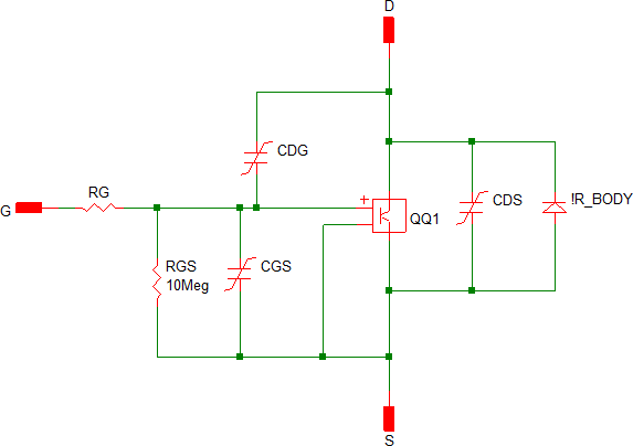
MOSFET - Level 2: Model Structure
In order to model the switching transitions of a MOSFET, you must use either a SIMPLIS MOSFET model Level 2 or 3. Since model Level 3 is just a very flexible user-defined extension of model Level 2, our main focus here is to learn how to become proficient at using model Level 2. In most cases, the Level 2 model will yield excellent results. The model structure of the SIMPLIS Level 2 MOSFET model is shown below.
| Level 2 models these circuit elements | Level 2 Schematic | ||||||||||||||
|
|
Each of the four supported MOSFET model levels are well documented here: SIMPLIS MOSFET Models
In the tabel below we compare the complexity of the four supported SIMPLIS MOSFET levels. The characteristics of the Level 2 model are highlighted in blue.
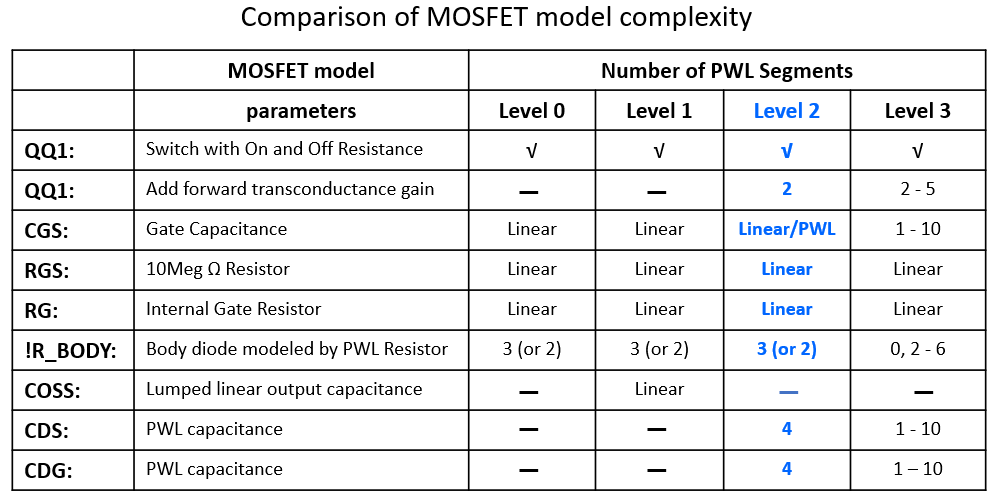
The MOSFET model Level 2 has been tuned over time to strike an attractive balance between simulation accuracy and simulation speed. All of the accuracy statements in this course have been achieved using model Level 2.
Unlike model Levels 0 and 1, in which all switching transitions occur instantaneously between an ON-resistance and an OFF-resistance, The Level 2 MOSFET model includes both the transconductance and the nonlinear capacitance. Model Level 2 models the transconductance of the active region of the MOSFET as the device transitions between ON and OFF. In addition, the model Level 2 captures the nonlinear behavior of the drain-to-gate capacitance and the drain-to-source capacitance. These two nonlinearities, especially the drain-to-gate capacitance, are critical in accurately modeling the switching transitions of a MOSFET in a switching power supply.
All levels employ an ON and OFF resistance. Level 2 models the forward transconductance gain of the active region as the MOSFET transitions from ON to OFF and from OFF to ON. The transconductance gain is modeled with two PWL segments in the drain current versus gate-to-source voltage plane as shown below.
In most devices the gate capacitance is quite linear. The Level 2 model extraction process tests the gate capacitance of the Spice MOSFET model. If the gate capacitance is nearly linear, a linear capacitor is used in the Level 2 model. If the gate capacitance is nonlinear, then a PWL capacitor is used. The body diode is modeled as a three (default) or two segment PWL resistor. Both CDG and CDS are modeled as 4-segment PWL capacitors.
At the user's discretion, the number of PWL segments may be increased using a Level 3 MOSFET model as shown in the last column of the table above.
Current Limitations of Model Levels 2 and 3
There are two notable limitations of the automated model extraction process for the SIMPLIS Level 2 MOSFET model.
- As will become evident in what follows, it can be important to model the nonlinear Drain-to-Gate capacitance CDG when it is negatively biased. In other words when vGS > vDS. Particularly with recent generations of MOSFET devices, CDG increases significantly when vGS > vDS. Our automated model extraction process in version 8.2 only measures and models CDG based on the forward biased voltage characteristics.
- Reverse recovery of the MOSFET body diode is not included in the automated MOSFET model extraction process as of version 8.2.
Despite these two model limitations, the results presented in our earlier discussion of in Module 1.0.4 Accuracy of PWL Models were all achieved with the MOSFET model extraction process available in version 8.2. Both of these limitations will be addressed in future versions of SIMetrix/SIMPLIS.
Data Sources
There are three main sources of information from which SIMPLIS MOSFET models are created.
- For discrete power MOSFETs, Spice Models are the most common source of information from which to extract and create a SIMPLIS MOSFET model. The automated SIMPLIS model extraction process takes advantage of the SIMetrix Spice simulator to run a number of Spice simulations on the Spice MOSFET model to draw the characteristic curves based on a user-defined operating range. The automated SIMPLIS model extraction process then does a PWL curve fit and extracts the SIMPLIS model parameters.
- If a good Spice model is not available, it is a straightforward process to create a SIMPLIS MOSFET model from graphical data sheet information. This comes primarily in the form of images from a .pdf file.
- Power Management IC suppliers may use internal MOSFETs as power switches, in which case, there is often neither a Spice model nor a data sheet. In this case, the characterization curves from a Cadence simulation using the foundry models can be used to initiate the SIMPLIS MOSFET model creation process.
As will be illustrated below, the primary limitation on the accuracy of the supported SIMPLIS Level 2 and 3 MOSFET models is the accuracy of the source information from which these models are created.
MOSFET Model Accuracy: Comparison with Spice
As mentioned in the introduction to this Application, when predicting MOSFET stresses and losses, it is as important to accurately model the MOSFET driver as to accurately model the MOSFET device itself. The nonlinear current limitations of the driver and the nonlinear behavior of the MOSFET contribute roughly equally to the shape of the MOSFET current and voltage waveforms during these switching transitions. This point is illustrated in the figure below.
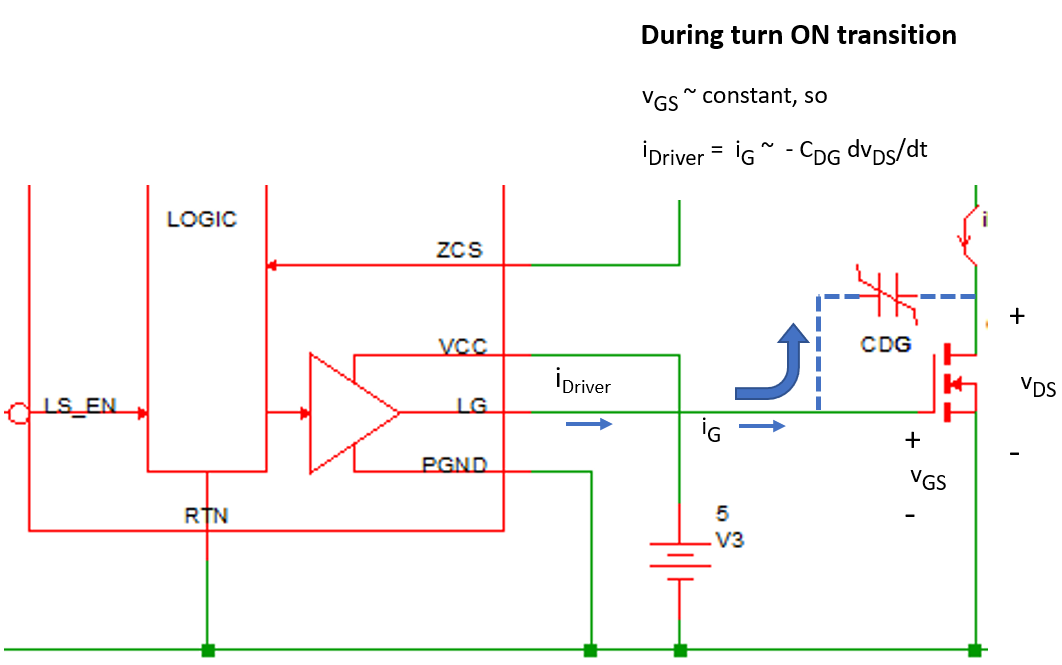
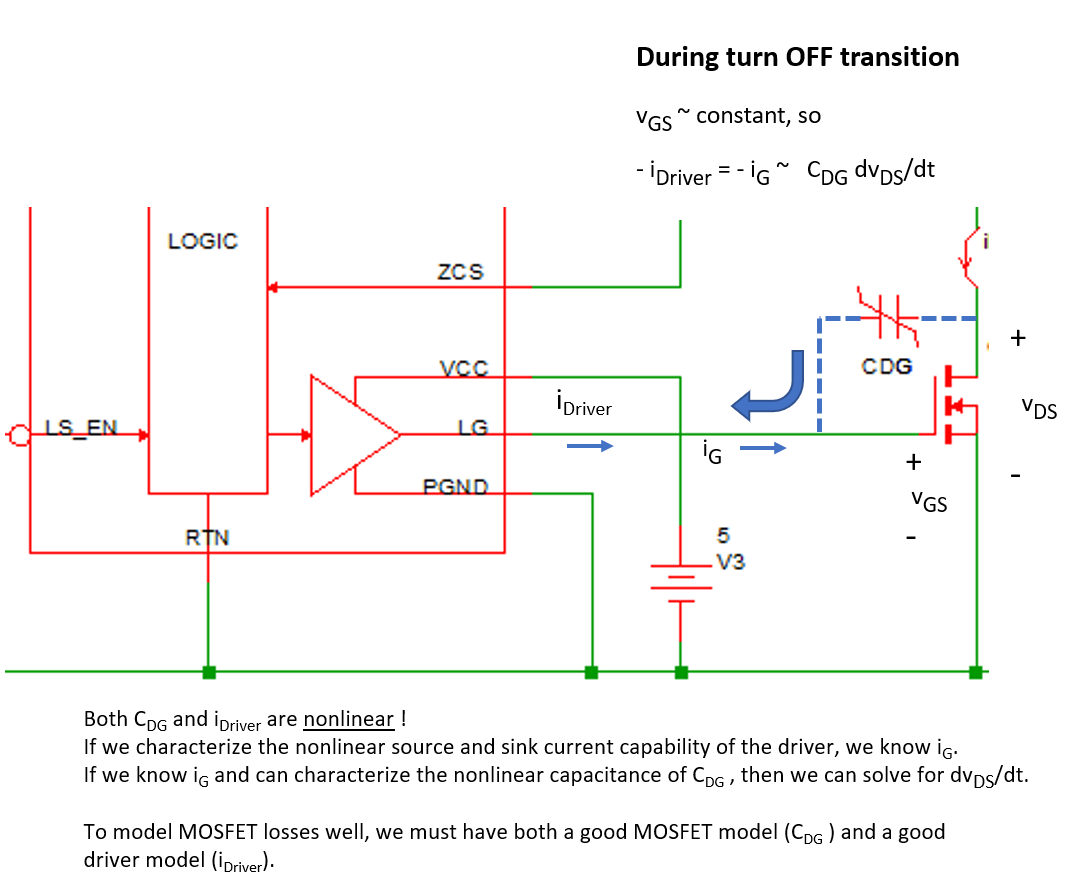
During the turn-ON transient of a MOSFET under an inductive load, the MOSFET current is essentially constant during the entire voltage transition from OFF to ON. Consequently, the gate voltage vGS is also nearly constant during the voltage transition of vDS. During this transition, the gate current iG = -CDG dvDG/dt ~ -CDG dvDS/dt. Since the driver current iDriver = iG, we can conclude that during the switching transitions, iDriver ~ -CDG dvDS/dt. As we have pointed out previously, the drain-to-gate capacitance CDG is highly nonlinear. So also is the driver current. However, if we can characterize both of these nonlinearities, we can predict with very high accuracy the shape of vDS during these switching transitions.
The same dynamic as what we just described for the turn ON transition controls the MOSFET turn OFF transition. By characterizing the nonlinear CDG and source and sink current limitations of the driver, we can accurately predict the voltage transition of vDS.
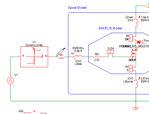
Even when we just seek to compare the behavior of Spice and SIMPLIS MOSFET models we must be extremely careful to have exactly the same test bench in both simulators. Begin by opening the testbench schematic for comparing a Spice MOSFET model with the same device modeled in SIMPLIS, apps_b_1_FDD8882_testbench.sxsch, which is shown below.
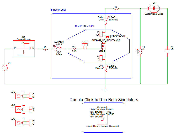
We first note that the Custom Ideal Diode D1 and the Current Limiter in the drive circuit are very carefully crafted to behave identically in both the SIMetrix Spice and SIMPLIS simulators. You may descend into this hierarchical schematic and discover how this was achieved and then verify that the behavior of U1 and D1 are indeed identical in both simulators. The Custom Ideal Diode D1 is modeled as a 2 segment PWL resistor with 100Meg Ohm OFF-resistance and 1m Ohm ON-resistance. The Current Limiter U1 in the gate drive circuit is modeled as a current limited voltage source with a 2 A current limit both when sourcing or sinking current.
The Spice model we use for comparison is the FDD8882 downloaded from the ON Semiconductor website. We then extracted a SIMPLIS Level 2 MOSFET model from this Spice model.
With the exception of one enhancement which we will discuss shortly, the simulation results presented here are exactly those that result from the downloaded FDD8882 Spice model and the extracted Level 2 SIMPLIS model.
Exercise #1: Compare Spice and SIMPLIS waveforms for FDD8882
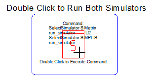
- First close your waveform viewer. Then double click on the red box with the letter S in its symbol to launch two simulations, the first in SIMetrix Spice and the second in SIMPLIS.
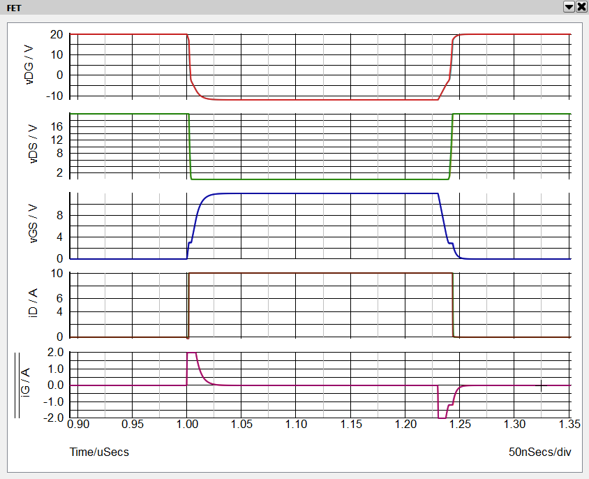
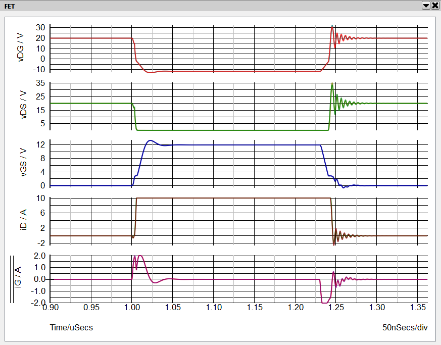
- In the waveform viewer go to the tab labeled "FET". Zoom in on the time axis to a time window of approximately t = 0.9 uS to t = 1.35 uS. From the top are displayed vDG, vDS, vGS, iD and iG.
Result: Note that the SIMetrix Spice and SIMPLIS waveforms are virtually indistinguishable at this zoom level.
- Next we need to point out some modifications to both the Spice model and the SIMPLIS model that were made to make it easier to visualize the current and voltage waveforms of this MOSFET device. Look back at our testbench schematic.
- Spice model: While no material changes were made to the FDD8882 Spice model, we did move some of the components around inside the testbench circuit. These moves make it much easier to visualize the detailed operation of the device during the turn ON and turn OFF transients. This is especially helpful when comparing the Spice and SIMPLIS model performance.
- The gate resistor RG was moved outside both MOSFET models.
- The lead inductances and their accompanying shunt resistors were also moved outside of the Spice model.
- We then inserted differential probes to measure the internal voltages vGS, vDS and vDG without including the lead impedances in these measurements.
- SIMPLIS model: We started with a Level 2 SIMPLIS model extracted from the FDD8882 Spice model. We then made the following changes:
- The gate resistor RG was moved outside of the MOSFET model.
- The lead inductances and their accompanying shunt resistors, not normally included in the SIMPLIS Level 2 model, were added externally and were given the identical values as those of the Spice model.
- We then manually added two segments to the PWL capacitor model for CDG to model its behavior when vDG is between 0 V and -10 V. As of version 8.2 the Level 2 MOSFET model extraction test only characterizes CDG when vGS is greater or equal to zero. This modification changed the agreement between the SIMPLIS model results and those of Spice from "pretty good" to outstanding.
- For the moment, we have effectively removed the lead inductance from both models by reducing the shunt resistor around each inductor to 1p Ohm. Once we have compared the waveforms without the lead inductance, we add the lead inductors back into both models and compare those results.
- Spice model: While no material changes were made to the FDD8882 Spice model, we did move some of the components around inside the testbench circuit. These moves make it much easier to visualize the detailed operation of the device during the turn ON and turn OFF transients. This is especially helpful when comparing the Spice and SIMPLIS model performance.
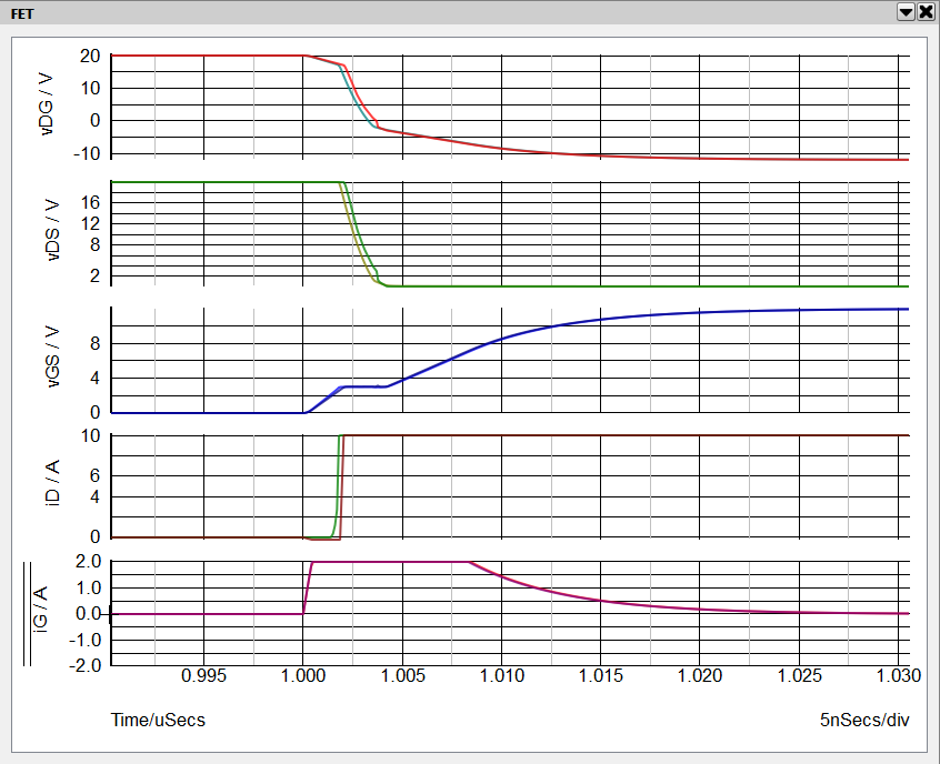
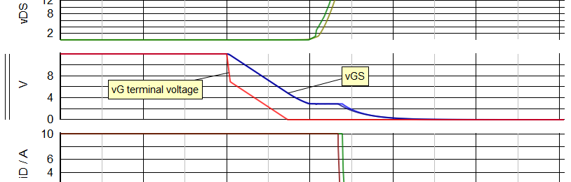
- Now zoom in to the turn-ON transient from about t = 0.99 uS to t = 1.03 uS. At this zoom factor we can discern some differences between the Spice and SIMPLIS voltage and current waveforms. However, they are minute and, as we demonstrate below, these differences contribute a negligible amount of error in the loss estimations.
- Observe that we can see the Miller plateau very clearly in the vGS waveform. Here is when the gate voltage vGS remains essentially constant during the vDS (or vDG) transition. It is during this interval that iG ~ -CDG dvDS/dt.
- Looking at the vDG and vDS waveforms we can clearly see the highly nonlinear nature of CDG. Looking at vDG during the interval when iG = 2A, we can see that CDG increases dramatically once vDG is less than about -1.5 V.
- Next zoom in to the turn-OFF transient from about t = 1.21 uS to t = 1.27 uS. Again we can see the Miller plateau on the vGS waveform during the vDS voltage transition.
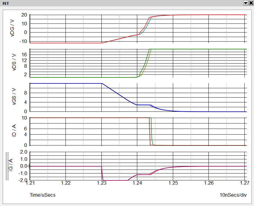
- Note: Note that, unlike during the turn-ON transition, during the turn-OFF transition the Miller plateau of the vGS waveform occurs not when iG is limited by the maximum current limit of the driver,but rather when iG is limited by the gate resistance RG of the MOSFET.As we shall see directly, this would be very difficult to ascertain if we included the gate resistor inside the MOSFET model and only had access to measure the gate terminal voltage.
- To illustrate this point, select the vGS grid.
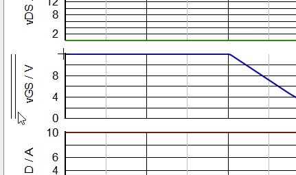
- Then randomly probe the gate terminal voltage as shown below. This probe point is all that would be accessible in a lab measurement.
- As we can see below, in this device, the voltage drop across the gate resistance RG is substantial during the turn OFF transient. We lose sight of much of what is actually happening on the gate of the device.
In the next Exercise, we look at a method to measure the switching losses in our testbench circuit.
Exercise #2: Compare Spice and SIMPLIS Loss predictions for FDD8882
In this exercise we look at two methods for measuring the losses in a switching MOSFET. The first method is simply to put a Power Probe on the device. With the second method we measure the total energy dissipated during each portion of the switching cycle, including both turn ON and turn OFF losses.
- Begin by closing your waveform viewer, if it is open. Reopen the testbench schematic apps_b_1_FDD8882_testbench.sxsch, and note that there is a power probe placed on our device under test QDUT.
A power probe measures the instantaneous power dissipated in the device. In a switching circuit, the average of the instantaneous power over an exact multiple of switching cycles will yield the correct power dissipation for that particular operating condition.
The other option when using a power probe is to employ the cursors in the waveform viewer to exactly prescribe an integral number of switching cycles and then take the average of the power dissipated in the device.
Because a major objective of our testbench is to have a single test circuit that will run with both the SIMetrix Spice and SIMPLIS simulators, we are constrained to only being able to run transient simulations. As a result, this testbench is set up to only run through one ON - OFF switching cycle. This is advantageous for comparing time domain current and voltage transient waveforms from both simulators, but it is not as effective for measuring dissipated power for periodic systems. As a result, we have chosen to measure the dissipated energy in QDUT during each portion of the single pulse test. We can then scale this result based on the anticipated switching frequency to arrive at a good estimate of average power dissipated.
The testbench circuit has four arbitrary probes that measure the following quantities:- Energy dissipated (integral of power dissipation) during turn ON interval
- Energy dissipated during conduction interval
- Energy dissipated during turn OFF interval
- Total energy dissipated entire single pulse transient simulation
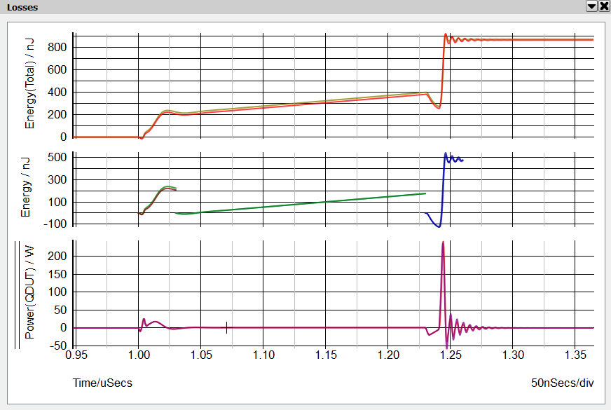
- Double click on the box with the red "S" to launch a simulation in both SIMetrix Spice and SIMPLIS. In the waveform viewer go to the tab labeled "Losses".
Here we see in the top grid the total energy dissipated during the course of the switching cycle. The middle grid shows the break out of the energy dissipated during the turn-ON transient, the conduction period and the turn-OFF transient. The last value of each curve is the result of the integral of the energy dissipated over its respective interval. The lower grid shows the instantaneous power dissipation of QDUT during this switching transient.
This approach is every effective in performing the comparison between the two MOSFET models. When you zoom into these waveforms you will be able to see the very slight differences between the Spice model and the SIMPLIS model. When taken over the entire switching transient, the differences between the Spice loss estimates and the SIMPLIS loss estimates are less than 0.5%. The difference in estimated conduction loss is ~ 1%. The differences in either turn-ON loss or turn-OFF loss are less than 2%.
Exercise #3: Enable Lead Inductance for FDD8882
Using the Load Component Values function we will restore the lead inductors to the Spice model and add them to the SIMPLIS model.
- From the menu bar, Select Tools > Load Component Values > Select a File to Load .
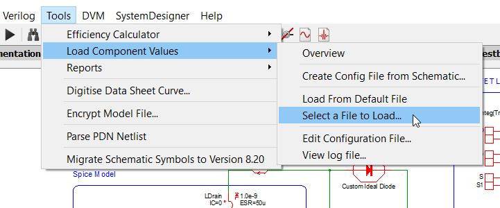
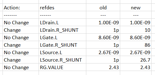
- Choose the LCV file named inductors_FDD8882.compvalues.txt
Result: Confirm that the following changes were made.
- Double click on the box with the red "S" to run the testbench in both simulators. Examine the voltage and current waveforms on the tab labeled "FET".
Result: Once we add all three lead inductors, the circuit becomes too complex for us to anticipate the precise shape of the MOSFET waveforms. None the less, we observe a remarkable degree of correlation between the Spice and the SIMPLIS simulation results.
- Now look at the energy loss waveforms on the tab labeled "Losses".
MOSFET Model Comparison - Summary
As we have seen in the Exercises above, the SIMPLIS PWL MOSFET model is capable of modeling the detailed behavior of MOSFET switching transitions. The SIMPLIS PWL MOSFET model yields excellent agreement with Spice when
- prediting the current and voltage time domain waveshapes, and
- estimating the energy lost during each portion of the switching cycle.
In the second scenario, we restore the lead inductors in the Spice model and add them to the SIMPLIS model. Again, outstanding agreement is observed. We conclude that the piecewise linear nature of the SIMPLIS simulator does not present fundamental or practical limitations in the accuracy with which we can predict MOSFET switching waveforms or losses.
As we explore further looking to predict switching losses in a closed-loop switching power supply, the piecewise linear nature of SIMPLIS actually has the advantage of having rather simple behavioral models for MOSFET devices that do not require highly-trained subject matter experts to create. In fact a good SIMPLIS MOSFET model can be created by hand from data sheet information in less than 30 minutes with just a little practice. As long as the data used to create the SIMPLIS MOSFET model is accurate, we can expect accurate results.
Before we jump into predicting switching losses in a closed-loop switching power supply, we need to first examine the critical aspects of the MOSFET driver that need to be modeled well in order to ensure accurate switching loss predictions.
MOSFET Driver Model
As discussed earlier, the nonlinear current limitations of the MOSFET driver and combine with the nonlinear capacitance CDG of the power MOSFET to dominate the shape of the vDS voltage transition. The shape of this voltage transition has a first order impact on the switching losses of a switching power supply.
- Open schematic file apps_b_2_buck_converter.sxsch. This is the schematic we will use to measure power stage losses in the following exercises.
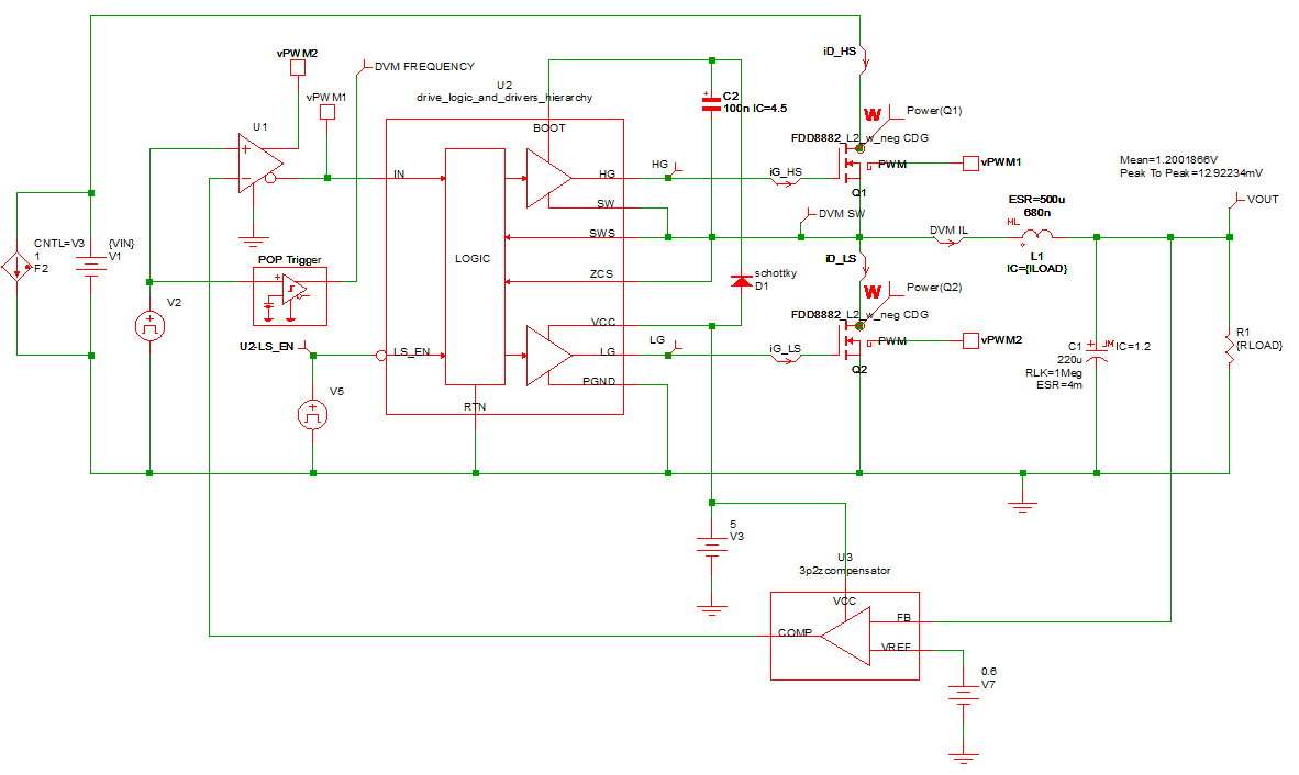 To start this discussion, we look at the key MOSFET driver parameters and where they are defined in this model.
 - Select the dual MOSFET driver symbol U2.
- Descend into the schematic subcircuit of this driver model.
- There are two SIMPLIS multi-level MOSFET driver blocks in this schematic. U2 in this subcircuit controls the drive signals for the high-side power MOSFET Q1 and U4 controls the drive signals for the low-side power MOSFET Q2.
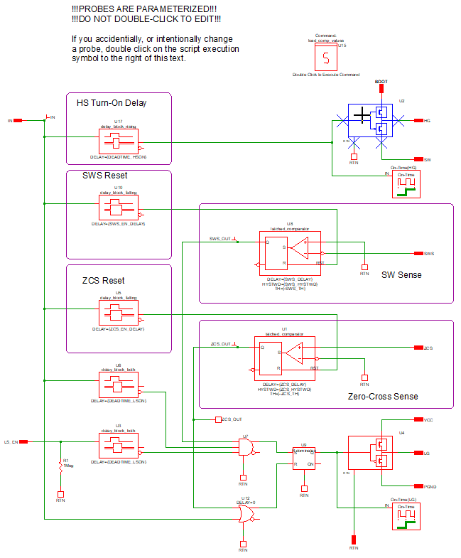
- Double click on U2, the multi-level MOSFET driver block.
- As described in detail below in Appendix B Characterizing the Multi-Level MOSFET Driver, this driver block when set to Level 1 conveniently allows the user to independently set the maximum source and sink current available from the driver as well as the series resistance of the driver devices when either sourcing or sinking current.
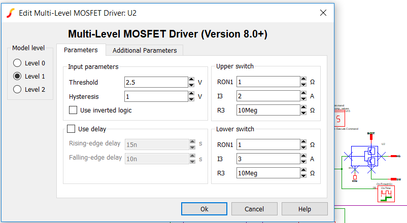
- As you can see from the Multi-Level MOSFET Driver dialog box, the maximum current that U2 can source is 2 A and the maximum current that it can sink is 3A. Note that the output series resistance is 1 Ohm in both source and sink modes. In this example, the driver block U4 is set up identically to U2.
- Run a simulation (press F9) on schematic apps_b_2_buck_converter.sxsch and look at the waveforms of the two gate currents iG_HS and iG_LS in the graph tab labeled "FET". Verify that the maximum source and sink currents of the high-side and low-side drivers are the same as defined in the Edit dialogs for the two multi-level drivers, U2 and U4, in the dual MOSFET driver subcircuit.
Measuring Power-Stage Losses
In this section, we describe two techniques to analyze the switching losses in a closed-loop synchronous buck dc-to-dc converter. We have already demonstrated that we can accurately model both the MOSFET power switches and the MOSFET drivers. Next we show two techniques to analyze switching losses in a complex MOSFET configuration within a closed-loop system.
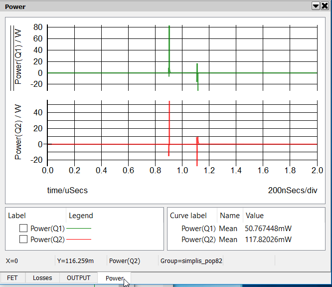
Put a Probe On It: The first technique is quite simply to put a power probe on each MOSFET of interest as shown in the schematic apps_b_2_buck_converter.sxsch. Each power probe displays a waveform showing the instantaneous power dissipation. Each power probe is set up to measure the average of the instantaneous power over the entire simulation.
In this case, we have set the schematic up for a Periodic Operating Point analysis displaying exactly one cycle of steady-state operation. Consequently, the average of our measurement is the same as the average MOSFET power dissipation at this operating condition.
Exercise #4: Measure MOSFET losses in closed-loop power supply
- Close the waveform viewer. Open schematic schematic apps_b_2_buck_converter.sxsch. Run the simulation (Press F9).
- In the waveform viewer select the graph tab labeled "Power".
Result: By setting up the POP analysis to display exactly one switching cycle and measuring the average value of the instantaneous power dissipated in both power switches, we can achieve an accurate, fast and repeatable prediction of the switching losses in this dc-dc converter.
- From the top level schematic apps_b_2_buck_converter.sxsch highlight the MOSFET symbol for Q1.
- Descend into this hierarchical schematic.
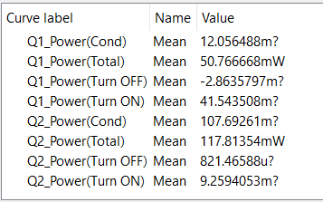
In the rectangular box labeled MOSFET Loss Analysis we have four arbitrary probes that measure power dissipated in the MOSFET. The probe on the bottom, labeled Power(Total) measures the total instantaneous power dissipated in the MOSFET over the entire simulation interval. By taking advantage of the POP analysis where we can arrange to present an exact integral multiple number of switching periods, in this case exactly one switching period, we can then easily measure the average of the instantaneous power dissipated in each power switch.
We can further break down the switch losses into Turn ON, Conduction and Turn OFF losses.
Measuring Switching Losses: Conclusions
- PWL MOSFET Level 2 models are as good as the source data - (see model limitations below)
- Virtually identical to Spice results
- Simple enough to create manually (~30 minutes)
- Data Sheet (.png images)
- Characteristic curves generated by Cadence from foundry models
- Can model key driver parameters very well and simply using SIMPLIS built-in parameterized driver models
- Datasheet
- Spice model characterization
- Hardware characterization
- Can model other major power stage components well
- Capacitors
- Diodes
- Magnetics (current and voltage waveforms)
- Current power stage component model limitations
- Reverse recovery model for diode is not supported by GUI or automated process.
- CDG reverse biased behavior is not included in automated Level 2 & 3 model extraction process
- Magnetics loss models in development
- Can simulate time domain closed-loop power supply
- Steady State (POP) analysis ideal for measuring/estimating losses
- Fast (Does not require long transient)
- Accurate (Does not require long transient)
- Repeatable (Does not require long transient)
- High resolution of key waveforms (data points / cycle)
- POP allows 1 cycle of steady state waveform output with maximum resolution
- All simulation time and data collection is useful
- Steady State (POP) analysis ideal for measuring/estimating losses
- Best Accuracy in Shortest Time