Voltage-Controlled Oscillator w/ Programmable Duty Cycle
The Voltage Controlled Oscillator (VCO) w/ Programmable Duty Cycle models a VCO with programmable ramp peak and valley voltages and a voltage-to-frequency gain. This block is speed-optimized for SIMPLIS simulations and can be used as a fixed frequency oscillator by connecting a constant DC voltage source to the frequency pin. This oscillator includes an ON/OFF control pin and outputs commonly used signals that include the following:
- Voltage ramp signal with programmable peak and valley voltages
- Clock signal with programmable duty cycle
- Output that can be converted into an analog counter that counts clock cycles
For a VCO with a 50% duty cycle, see the Voltage-Controlled Oscillator w/ 50% Duty Cycle topic.
In this topic:
| Model Name: | Basic Voltage-Controlled Oscillator | |
| Simulator: | This device is compatible with the SIMPLIS simulator. | |
| Parts Selector Menu Location: | ||
| Symbol Library: | simplis_analog_functions.sxslb | |
| Model File: | simplis_analog_functions.lb | |
| Subcircuit Name: | SIMPLIS_OSC101_BB | |
| Symbols: | 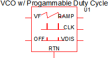
|
|
| Multiple Selections: | Multiple devices can be selected and edited simultaneously. | |
Previous Version Compatibility
This symbol was introduced with version 8.0; however, the model and supporting files are available in version 7.20 as well. In versions prior to 7.20, the schematic will simulate, but you will not be able to edit the parameters with the dialog pictured in this topic.
For a version of the VCO compatible with versions prior to version 7.20, see the parts selector entry:
Symbol Migration
Symbols placed on schematics in previous versions of SIMetrix/SIMPLIS can be automatically migrated to use the new symbols. The schematic tools menu will invoke a routine which migrates the existing symbols to the new symbols. As this action makes substantial changes to the schematic, it is recommended that you save a backup copy of the schematic first.
I/O Table
The following table describes the pins on the VCO symbol.
| Pin_Name | I/O | Function | Description |
| VF | I | Input voltage that controls the clock frequency. | \[ f_{CLK} = VF \times Gain \]
where ???MATH???Gain???MATH??? is the clock frequency when VF = 1.0 |
| OFF | I | On/Off control voltage for the oscillator | Oscillator runs when the OFF
voltage signal is less than 2.0V.
|
| RTN | The circuit return for the VCO | The ground reference for this circuit | |
| RAMP | O | Saw tooth ramp voltage output | This output allows you to
probe the internal oscillator ramp voltage.
|
| CLK | O | Digital logic output Logic
0 => CLK = 0V |
The clock frequency is controlled by the VF input. The clock parameters are set in the input dialog box described in Editing_the_VCO. |
| V_DICH | O | V_DICH output voltage |
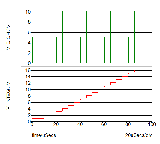
V_DICH provides output voltage signal. When this output is connected as shown in the schematic example below, the V_INTEG signal is proportional to the number of clock cycles. |
Editing the VCO
To configure the VCO, follow these steps:
- Double click the symbol on the schematic to open the editing dialog.
- Make the appropriate changes to the fields described in the table below the image.
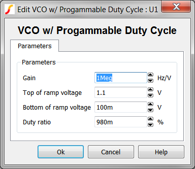
Label Parameter Description Gain The gain of the VCO is described in Hz/V.
A VCO with a Gain parameter value of 100k will oscillate at 100kHz when the VF pin voltage is 1V. When the VF pin is 5V the same VCO will oscillate at 500kHz.Top of ramp voltage The peak of the ramp voltage Bottom of ramp voltage The valley of the ramp voltage Duty ratio The ramp duty cycle. The clock pin will have a duty ratio of:
\[ D_{CLK} = 1 - Duty ratio \]
Examples
The test circuit used to generate the waveform examples in the next section can be downloaded here: simplis_070_vco_programmable_duty.
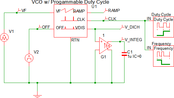
Waveforms
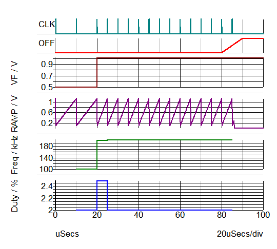
The waveforms shown below are for a test circuit with the following characteristics:
- The VF pin changes between 0.5 and 1V at 20us.
- The resulting oscillator frequency changes from 500kHz to 1MHz.
- The OFF pin is asserted with a PWL voltage ramp starting at 80us.
- The oscillator turns off when the OFF pin voltage crosses the 3V threshold.
The waveform below shows the integrator output proportional to the number of clock cycles. The V_INTEG voltage increases 1V for every oscillator cycle.